PIEZO NANOPOSITIONING BASICS
Learn About Nanopositioners & How to Select the Best Piezo Stage

Learn the fundamentals of piezo nanopositioners and learn how to select the best piezo stage for your application.
QUICK NAVIGATION:
- What is the Piezo Effect?
- What is a Piezo Actuator or PZT?
- What is the range of motion of a typical piezo device?
- Properties Guide of Piezo Actuators
- Different Control Systems for Piezo Actuators
- Analog Control Systems for Piezo Stages
- Digital Feedback Control Systems for Piezo Stages
- Applications for Piezo Stages
- Where to Find Piezo Stages?
A new world in positioning and alignment to the nanometer level has been enabled by piezo actuators providing nano-level motion in a variety of mechanisms and devices, even a piezomotor providing linear actuation with step sizes as low as 1 nanometer. Think about that, travel ranges in the millimeter range with step sizes as small as 1 nanometer. Not only that, but piezo actuators are capable of high forces and capable of moving loads of tens to hundreds of Newtons. Check out this video by PiezoMotor Inc,
What is the Piezo Effect?
Ok, small displacements with ever so smaller resolutions, you may be wondering how does that happen? The Piezo effect is an electrical charge that accumulates in a solid (ferroelectric) material in response to applied mechanical strain. It was discovered more than a hundred years ago, 1880 to be exact, but who’s counting?! Additionally, and most importantly for our world in nanopositioning, the piezoelectric effect is a reversible process; ferroelectric materials exhibit the internal generation of a mechanical strain resulting from an applied electrical field. Hence, the creation of an industry in nanopositioning.
For those interested in the origins of the terminology; piezoelectric is derived from the Greek word piezein, which means to squeeze or press, and ēlektron, an electric charge.
What is a Piezo actuator or PZT?
Enough of the background, let’s get down to business. Piezo actuators are simple devices conceptually and are made of layers of thin ferroelectric materials 10’s of microns thick, typically made from lead, zirconium and titanium (often referred to as lead zirconate titanate) and interleaved with electrodes for activation of the effect. Consequently, they are often called piezoelectric transducers, or PZTs – an acronym which reflects their elemental constituents (look at the Periodic Table, Lead (Pb), Zirconium (Zr) and Titanium (Ti)). You may be asking, there are no ferro based materials (iron for example) in these devices, what’s the deal with ferro in ferroelectric? The term ferroelectric came out of the discovery of the piezo principle (a spontaneous electric polarization) analogous to the well- known (at the time of discovery) ferromagnetic materials (inherent magnetic polarization).
Simply and more importantly, these actuators change their respective dimension when an electric field (voltage) is applied across them. No moving parts, no bearings, solid state frictionless action! They produce precise nanomotion, high forces and very short response times. They are typically configured in linear stacks, stacked stages, flexure guided actuators, providing a wide range of linear motion in singular or X-Y planes respectively. Piezo motors also provide rotational motion with high angular velocity and less than 1 arc-second resolution; that is 0.0023 degrees!
What is the range of motion of a typical piezo device?
Think small, smaller and even smaller! Stacked piezo actuators are designed to provide motion ranges of 5 to 300 μm. It’s difficult enough to see one millimeter, these ranges are 100 to 1000 times smaller! This electrically induced dimensional change is typically on the order of 0.13% of the devices original dimension meaning a 100-mm-long stack can expand to 130 μm when the maximum allowable voltage is applied. Benders, where the electric field induces a bending motion, think of a cantilever, (as opposed to contraction or expansion in stacks) produces displacements in the millimeter range. Flexure actuators provide precision guided motion with displacements also in the millimeter range. Piezo linear motors or “walking” motors are an incredible technology with large displacements in the 10’s of millimeter range. Not bad considering the resolution in the nanometer realm!!
You can learn more about the design and control of these piezo stages from the paper Design Methodologies for Robust Nanopositioning by Abu Sebastien and d Srinivasa M. Salapaka.
A quick basic properties guide of Piezo Actuators
You get it, cool technology where an applied voltage can cause nanometer displacements in specific materials. Is that all there is? No, there’s much more. To understand the data sheet for these piezo stages and nanopositioners it is good to have an overview of the specifications.
» High Resolution - The piezo ceramic itself works free of friction, the resolution attainable is a function of control electronics and mechanical parameters in design and mounting.
» High Force Generation - You are not going to believe this, high load piezo actuators are capable of moving loads of several tons, probably on the unusual side, the point is they can move high loads, 10’s to 100’s of Newtons typically with resolutions in the nanometer range!!
» High Speed - The speed of piezo actuators comes from the solid state actuation of the material in response to an electric field which propagates through a stack at the speed of sound! This translates into response times in microseconds.
» High Stiffness - Typical actuators have stiffnesses between 1 and 2,000 N/μm and compressive limits between 10 and 100,000 N. This makes sense, consider taking a solid material and stretching (or compressing it), like a very stiff spring.
» Voltage Operated - Two types of piezo actuators operate over a wide range of control voltages. Monolithic low voltage multi-layered actuators made of ceramic layers from 10 to 100 μm operate at voltages up to 130 volts. High power actuators made from ceramic layers 0.5 to 1 mm thick operate at voltages up to 1000V.
» No Wear and Tear - A piezo actuator has no moving parts, Piezo actuators have gone through billions of cycles in endurance tests without measurable changes in their behavior.
» Low Energy Consumption - Static operation even while holding heavy loads for long periods consumes virtually no power, the device acts much like an electrical capacitor, an energy storage device! No heat is generated, no energy loss. In other words high efficiency!
You can’t just tweak a micrometer for nanopositioning systems, what about the controls for these systems?
Well you could try, but you wouldn’t be happy with the results or the time to get down to positioning in the nanometer range! An important point to remember when working with piezo devices is that they are voltage controlled, the point being that for piezo stack actuator-driven positioners, the drive signal from the controller operates in the position domain, that is nanometer position range! This necessitates high-quality, low-noise, low-drift circuit design for the servo circuit, be it analog or digital. In addition, the high responsiveness (discussed earlier) of piezo actuators necessitates very fast processing. The controls for these devices is a very critical decision and will determine the success or failure of your piezo-based system.
Here is a quick summary of analog and digital controllers, system requirements will dictate which is best suited for your application. Certainly, more information is needed than is offered here and there is a wealth of information available to help choose the control system on.
A good detailed discussion on Piezo Control can be found on the PI blog website.
Good old Analog Control, it just won’t go away (nor should it)
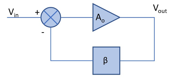
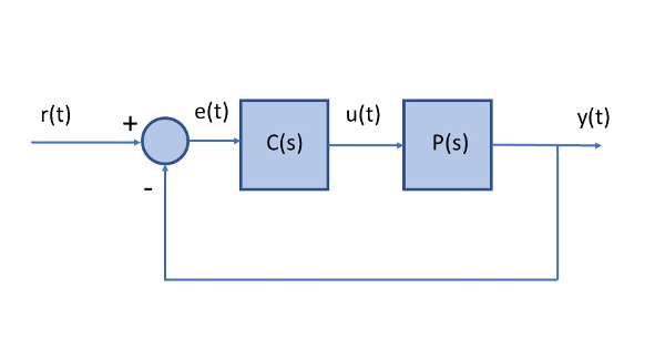
Traditional (analog) nanopositioning controller designs utilize sensitive op-amp circuits to implement the familiar proportional-Integral feedback-driven servo. The job of the servo is to reduce the difference between the command signal (generally a voltage generated by a DAC elsewhere in the controller or on a card in the user’s PC) and the feedback signal from the position sensor embedded in the motion device. However, these architectures are sensitive and prone to DAC drift and induced noise through system connections resulting in position instability. System calibration changes due to load changes would require adjustments typically using trim pots. Costly and inefficient!!

The New Digital Control, the best of both worlds.
By comparison, digital controllers implement servo functionality through DSP (digital signal processing) rather than in analog circuitry. This true-digital architecture allows the DAC to be integrated inside the servo loop. And DAC drift can be virtually eliminated since the system intelligence can differentiate between desired and undesired motions.
True digital controllers offer dynamic settings that can be easily changed remotely via software and then safely stored to the unit’s flash RAM. Optimized dynamic parameters can be downloaded to the controller at any time without requiring physical access to the unit or even a power-cycle. This capability allows easy optimization for momentary application requirements in addition to configuration changes, such as a new load. This means the nonlinearity of strain sensors can now be affordably addressed by real-time digital compensation, providing up to a 10X improvement in absolute accuracy.

Where are these devices used?
You may be surprised by the many different and interesting applications of piezo based devices which date back to the early 1900’s where they were developed to detect submarines during WWI, crystals used in radios allowing aircraft fighters to communicate during WWII, and are now used in the production and detection of sound, generation of high voltages, and electronic frequency generation, to drive an ultrasonic nozzle.
Piezo Stages are used in applications requiring precise nanometer motion and control. Common Applications are:
» Beam Adjustment - Nanometer adjustment in the optical systems allows for precise beam adjustment in a range of laser systems.
» Beam Tracking - In biological applications were a laser is focused on to a cell nanometer resolution is required to maintain the laser on the cell.
» Microscope Inspection - In particular metrology applications and semiconductor inspection the precise motion of the sample is required for accurate inspection.
» Atomic Force Microscopes (AFM) - Require stable and precise motion in order to accurate measure the sample. The piezo stage is ideal for this application with both the precise motion and speed. A paper by William S. Oates and Ralph C. Smtih title Nonlinear Control Design for a Piezoelectric Driven further explores this topic.
More indepth discussion of Piezo Stage and Nanopositioning Applications can be found from PiezoSystems Jena.
Finding a piezo stage for my demanding nanopositioning application.
So you have determined that you need to have motorized sub nanometer movement and no other option will work for you. Luckily our free and open product index allows you to research and compare all the suppliers of Piezo Stages right here.